Nanofabrication of lasers and photonic structures
The fabrication of organic lasers made in our group involves a few simple steps.
The resonators used for our organic lasers are normally periodic diffraction structures:
Distributed feedback resonators (DFB) – Periodic one dimensional (1D) or two dimensional (2D) gratings. Feedback is provided by the Bragg diffraction of the travelling waves from the gratings at certain wavelengths.
Distributed feedback reflectors (DBR) – Consisting of a central flat gain region and two Bragg diffraction grating regions serving as the reflective mirrors. The lasing modes are chosen among the longitudinal modes supported in the centre gain region by the stop band of the Bragg mirrors.
These resonators can be fabricated by the following methods:
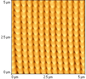
Electron beam lithography – This produces high quality small scale resonators up to 100 micrometers in size. The gratings are first made on a photoresist (e.g. PMMA) coated on a silica substrate. Exposure to the electron beam under very high vacuum leads to cross linking inside the photoresist, which records the grating patterns. After exposure, the resist is developed in a developer to form the gratings. The shortest period achieved is below 200 nm. The depth of the grating is determined by the exposure dose, such as the energy of the electron beam and the exposure time.
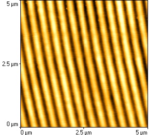
Holography – This technique is useful for large scale resonators (100 micormeters – 10s of millimeters). The photoresist is usually SU-8 (negative resist) or SR 1805 (positive resist), both of which are very sensitive to the UV light. The gratings are determined by the two beam interference patterns from the laser beam, followed by the similar cross linking and developing process. The shortest period with relatively high quality we have created is close to 280 nm. After being developed, the sample is place inside an RIE machine which can etch the grating from photoresist into the silica substrate.
Once the corrugated silica substrate is made, to make a organic laser, a layer of active material can be directly spin coated onto the substrate or the substrate can be used as a master to transfer the gratings onto the laser gain medium coated on a flat silica substrate. The latter case is more efficient in terms of mass production of organic lasers. There are several ways to realize grating transfer:
Soft lithography– This is a cost effective approach to transfer the pattern at room temperature. First, a plastic mould (PDMS or copolymer) should be made based on the corrugated substrate. Wet by the organic solvents used to dissolve the gain material, the mould is then put on top of the organic layer coated on a flat substrate with light pressure for two minutes. The final step is to peel the mould away from the organic layer. After these three steps, the grating can be successfully transferred. Usually, the depth of the transferred grating is smaller than the original grating due to the evaporating of the organic solvent.
Hot embossing
Nanoimprint lithography